Could stretching a thin crystal create a better solar cell?
June 26, 2015
This colorized image shows an ultra-thin layer of semiconductor material stretched over the peaks and valleys of part of a device the size of a pinkie nail. Just three atoms thick, this semiconductor layer is stretched in ways to enhance its electronic ability to absorb solar energy. The image is enlarged 100,000 times. (credit: Hong Li, Stanford Engineering)
Stanford University researchers have stretched an atomically thin Molybdenum disulfide (MoS2) semiconductor crystal to achieve a variable bandgap (defined as the amount of energy it takes to move an electron in a material).
That could lead to solar cells that absorb more energy from the sun by being sensitive to a broader spectrum of light, and could also find applications in next-generation optoelectronics.
Crystalline semiconductors like silicon can also catch photons and convert their energy into electron flows in solar cells, but they have a single band gap, which limits their absorption to a narrow region of the spectrum.

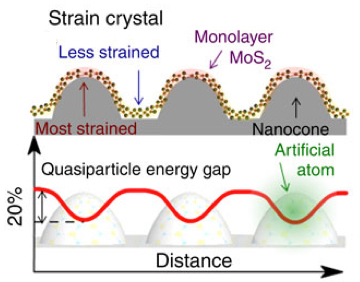
Schematic of strained MoS2 crystal (yellow) caused by indentations from SiO2 nanocones (gray). The stretched regions (on the tips of nanocones) have the highest tensile strain and the lowest band (energy) gap, while the areas between nanocones are less strained, so they have the highest band gap. This broad range of band gaps results in absorption of light over a broader spectrum. (credit: Hong Li/Nature Communications)
Stanford researchers reveal the details of this study in an open-access paper published in Nature Communications. MIT, Rice University, and Texas A&M University researchers also contributed to the paper.
Abstract of Optoelectronic crystal of artificial atoms in strain-textured molybdenum disulphide
The isolation of the two-dimensional semiconductor molybdenum disulphide introduced a new optically active material possessing a band gap that can be facilely tuned via elastic strain. As an atomically thin membrane with exceptional strength, monolayer molybdenum disulphide subjected to biaxial strain can embed wide band gap variations overlapping the visible light spectrum, with calculations showing the modified electronic potential emanating from point-induced tensile strain perturbations mimics the Coulomb potential in a mesoscopic atom. Here we realize and confirm this ‘artificial atom’ concept via capillary-pressure-induced nanoindentation of monolayer molybdenum disulphide from a tailored nanopattern, and demonstrate that a synthetic superlattice of these building blocks forms an optoelectronic crystal capable of broadband light absorption and efficient funnelling of photogenerated excitons to points of maximum strain at the artificial-atom nuclei. Such two-dimensional semiconductors with spatially textured band gaps represent a new class of materials, which may find applications in next-generation optoelectronics or photovoltaics.