How curly nanowires can absorb more light to power nanoscale electronic circuits
September 11, 2015

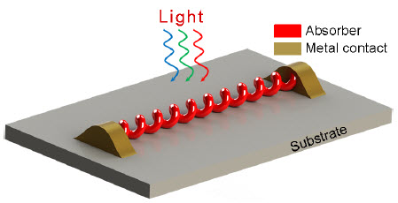
This illustration shows a prototype device comprising bare nanospring photodetectors placed on a glass substrate, with metal contacts to collect charges (credit: Tural Khudiyev and Mehmet Bayindir/Applied Optics)
Researchers from Bilkent University, Ankara, Turkey, have shown that twisting straight nanowires into springs can increase the amount of light the wires absorb by up to 23 percent. Absorbing more light is important because one application of nanowires is turning light into electricity, for example, to power tiny sensors instead of requiring batteries.
If nanowires are made from a semiconductor like silicon, light striking the wire will dislodge electrons from the crystal lattice, leaving positively charged “holes” behind. Both the electrons and the holes move through the material to generate electricity. The more light the wire absorbs; the more electricity it generates. (A device that converts light into electricity can function as either a solar cell or a photosensor.)
In 2007, U.S. researchers introduced a single nanowire photosensor that produced enough electricity from sunlight (up to 200 picowatts) to power nanoscale electronic circuits. More recently, a European researcher team built a nanowire solar cell with almost 14 percent efficiency from the compounds of indium and phosphorus. This efficiency is not enough to beat the best crystalline silicon solar cells on the market, but because nanowires can cover more area with less material, the nanowire solar cells could ultimately be cheaper.
“There is huge potential in the area of nanoscale photosensors,” said Mehmet Bayindir, Director, National Nanotechnology Research Center, Bilkent University. “More efficient outputs might induce the emergence of a new generation of photosensor technology and eventual commercialization of these products.”
Mie resonances increase current flow
Bayindir and his colleague Tural Khudiyev, now a postdoctoral associate at The Massachusetts Institute of Technology, have found that adjusting the geometry of the typical nanowire may be one way to realize the desired efficiency enhancement.
Nanowires are usually long, thin and straight. Their tiny dimensions mean they interact with light differently than ordinary materials. Certain wavelengths of light will match up in just the right way with the dimensions of the nanowire, causing the light to “resonate” or bounce around inside the wire.
These “Mie resonances” are especially advantageous at the nanoscale, Khudiyev said. The resonances are named after the early-20th-century German physicist Gustav Mie, who developed equations to describe why tiny metal particles make stained glass windows glow so brightly.
Mie resonances will occur with straight nanowires, but by twisting the nanowire into a helical shape, the researchers found they could take double advantage of the phenomena. “When the nanospring period matches the Mie resonance points, a ‘double resonance’ condition occurs, which boosts light harvesting efficiency,” Khudiyev said.
Additionally, twisting the wire upwards shortened its length, reducing the required area by up to 50 percent.
Nanoscale sensors
The enhanced light harvesting efficiency of nanosprings opens new opportunities to build nanoscale devices that power themselves, such as sensors to detect environmental toxins or to monitor the structural integrity of a bridge.
“Our nanospring shape induces more power output both in the broad spectrum range and at some desired single point (which can be engineered easily), and these make powering of more advanced nanosystems possible with a single nanospring-based photovoltaics system,” Khudiyev said.
“Experimental observation of a nanospring-based photosensor design and its integration into a large-scale fiber embedded system would be interesting as the next steps,” Bayindir said.
The group has already developed an easy way to produce nanosprings by first making long nanowire arrays, then heating them to a temperature at which the arrays can be twisted into the nanospring shape. The technique can be varied to control the diameter of the spring and the tightness of the curl.
The results of this research are published in the journal Applied Optics, from The Optical Society (OSA).
Abstract of Nanosprings harvest light more efficiently
Nanotechnology presents versatile architectural designs for the purpose of utilization as a building block of 1D optoelectronic nanodevices because current nanowire-based schemes require more effective solutions for low absorption capacity of nanoscale volumes. We report on the potential of nanospring absorbers as an alternative light-harvesting platform with significant advantages over conventional nanowires. Absorption capacity of nanospring geometry is found to be superior to cylindrical nanowire shape. Unlike nanowires, they are able to trap a larger amount of light thanks to characteristic periodic behavior that boosts light collection for the points matched with Mie resonances. Moreover, nanospring shape supplies compactness to a resulting device with area preservation as high as twofold. By considering that a nanospring array with optimal periods yields higher absorption than individual arrangements and core-shell designs, which further promote light collection due to unique antireflection features of shell layer, these nanostructures will pave the way for the development of highly efficient self-powered nanosystems.