How to turn a crystal into an erasable electrical circuit
August 4, 2017

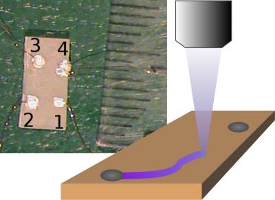
Washington State University researchers used light to write a highly conducting electrical path in a crystal that can be erased and reconfigured. (Left) A photograph of a sample with four metal contacts. (Right) An illustration of a laser drawing a conductive path between two contacts. (credit: Washington State University)
Washington State University (WSU) physicists have found a way to write an electrical circuit into a crystal, opening up the possibility of transparent, three-dimensional electronics that, like an Etch A Sketch, can be erased and reconfigured.
Ordinarily, a crystal does not conduct electricity. But when the researchers heated up crystal strontium titanate under the specific conditions, the crystal was altered so that light made it conductive. The circuit could be erased by heating it with an optical pen.

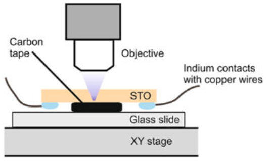
Schematic diagram of experiment in writing an electrical circuit into a crystal (credit: Washington State University)
The physicists were able to increase the crystal’s conductivity 1,000-fold. The phenomenon occurred at room temperature.
“It opens up a new type of electronics where you can define a circuit optically and then erase it and define a new one,” said Matt McCluskey, a WSU professor of physics and materials science.
The work was published July 27, 2017 in the open-access on-line journal Scientific Reports. The research was funded by the National Science Foundation.
Abstract of Using persistent photoconductivity to write a low-resistance path in SrTiO3
Materials with persistent photoconductivity (PPC) experience an increase in conductivity upon exposure to light that persists after the light is turned off. Although researchers have shown that this phenomenon could be exploited for novel memory storage devices, low temperatures (below 180 K) were required. In the present work, two-point resistance measurements were performed on annealed strontium titanate (SrTiO3, or STO) single crystals at room temperature. After illumination with sub-gap light, the resistance decreased by three orders of magnitude. This markedly enhanced conductivity persisted for several days in the dark. Results from IR spectroscopy, electrical measurements, and exposure to a 405 nm laser suggest that contact resistance plays an important role. The laser was then used as an “optical pen” to write a low-resistance path between two contacts, demonstrating the feasibility of optically defined, transparent electronics.