Imaging electric fields of molecules or atoms at sub-nanoscale
July 7, 2015

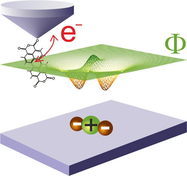
Illustration of the measuring principle: depending on the local electric potential (voltage) field of a nanostructure on the surface of a sample molecule or atom (bottom), a single electron (red) in a sensor molecule attached to the tip of an atomic force microscope (AFM) jumps from the tip of the microscope to the sensor molecule or not (credit: Forschungszentrum Jülich)
Using a single molecule attached to an atomic force microscope (AFM) as a more sensitive sensor, scientists in Forschungszentrum Jülich in Germany have used a new “scanning quantum dot microscopy” method to image electric potential fields (voltages) of electron shells of single molecules and even atoms with high precision for the first time, providing contact-free information on the distribution of charges.
The breakthrough technique is relevant for diverse scientific fields including investigations into biomolecules and semiconductor materials.
“Our method is the first to image electric fields near the surface of a sample quantitatively with atomic precision on the sub-nanometer scale,” says Ruslan Temirov from Forschungszentrum Jülich. Such electric fields surround all nanostructures like an aura. Their properties provide information, for instance, on the distribution of charges in atoms or molecules.
For their measurements, the Jülich researchers used an atomic force microscope. This device functions a bit like a record player: a tip moves across the sample and pieces together an image of the properties of the surface. Its limitation is that the large size difference between the tip and the sample causes resolution difficulties — imagine that a single atom is the size as a head of a pin; the tip of the microscope would then be as large as the Empire State Building.

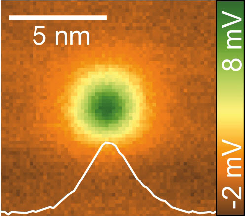
A single silver atom (green-yellow) on a silver substrate under the scanning quantum dot microscope (credit: Forschungszentrum Jülich)
Single quantum dot molecule functions as sensor
To improve resolution and sensitivity of the AFM, the scientists attached a single molecule as a “quantum dot” to the tip of the microscope. Quantum dots are tiny nanocrystal structures, measuring no more than a few nanometers across, which due to quantum confinement can only assume certain, discrete states comparable to the energy level of a single atom, making them ideal as a sensor.
The molecule at the tip of the microscope functions like a beam balance (measuring scale) that tilts to one side or the other. A shift in direction corresponds to the presence or absence of an additional electron, which either jumps from the tip to the molecule or does not. (The balance does not compare weights; it is affected by two electric fields that act on the mobile electron of the molecular sensor: the first is the field of a nanostructure being measured, and the second is a field surrounding the tip of the microscope, which carries a voltage.)
“The [bias] voltage at the tip is varied until equilibrium is achieved. If we know what voltage has been applied, we can determine the [electric potential] field of the sample at the position of the molecule,” explains Dr. Christian Wagner, a member of Temirov’s Young Investigators group at Jülich’s Peter Grünberg Institute (PGI-3). “Because the whole molecular balance is so small, comprising only 38 atoms, we can create a very sharp image of the electric field of the sample. It’s a bit like a camera with very small pixels.”
A patent is pending for the method, which is particularly suitable for measuring rough surfaces, such as in semiconductor structures for electronic devices or folded biomolecules.
“In contrast to many other forms of scanning probe microscopy, scanning quantum dot microscopy can even work at a distance of several nanometers. In the nanoworld, this is quite a considerable distance,” says Wagner. The technique has so far only been applied in high vacuum and at low temperatures, which are required to attach the single molecule to the tip of the microscope. “In principle, variations that would work at room temperature are conceivable,” suggests Wagner.
He says other forms of quantum dots could also be used as a sensor in place of the current molecule, using semiconductor material, such as quantum dots made of nanocrystals like those already being used in fundamental research.
The research results have been published in an open-access paper in the current issue of Physical Review Letters.
Abstract of Scanning Quantum Dot Microscopy
We introduce a scanning probe technique that enables three-dimensional imaging of local electrostatic potential fields with subnanometer resolution. Registering single electron charging events of a molecular quantum dot attached to the tip of an atomic force microscope operated at 5 K, equipped with a qPlus tuning fork, we image the quadrupole field of a single molecule. To demonstrate quantitative measurements, we investigate the dipole field of a single metal adatom adsorbed on a metal surface. We show that because of its high sensitivity the technique can probe electrostatic potentials at large distances from their sources, which should allow for the imaging of samples with increased surface roughness.