Japanese paper art inspires new 3-D fabrication method that goes beyond 3-D printing limitations
September 14, 2015

A new assembly method based on an ancient Japanese paper art quickly transforms 2-D structures into complex 3-D shapes. The results, reported by a Northwestern University and University of Illinois research team, could be useful in tissue engineering and microelectromechanical systems. (credit: University of Illinois)
A research team has created complex 3-D micro- and nanostructures out of silicon and other materials used in advanced technologies by employing a new assembly method that uses a Japanese Kirigami paper-cutting method.
The method builds on the team’s “pop-up” fabrication technique — going from a 2-D material to 3-D in an instant, like a pop-up children’s book — reported in January this year on KurzweilAI and in the journal Science. Those earlier ribbon-like structures yielded open networks, with limited ability to achieve closed-form shapes or to support more complex spatially extended devices.
In their new work, the research team at Northwestern University, University of Illinois and Tsinghua University solved this problem by borrowing ideas from Kirigami, the ancient Japanese technique for forming paper structures by folding and cutting. The Kirigami study was published last week (Sept. 8) in the Proceedings of the National Academy of Sciences (PNAS).

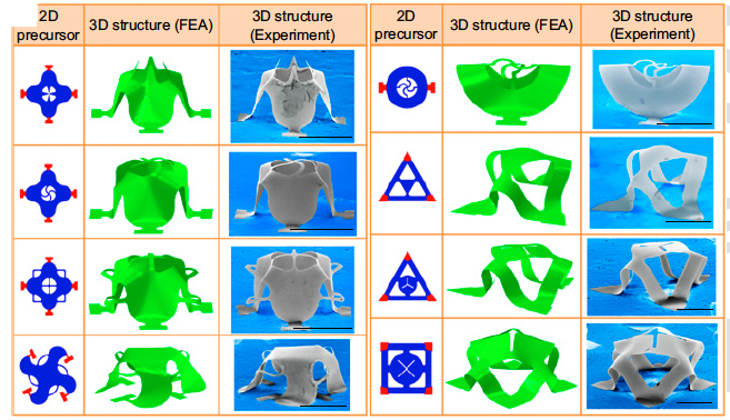
Two-dimensional precursors, finite-element analysis predictions, and scanning electron microscope images for five 3-D membrane–ribbon hybrid mesostructures (credit: Yihui Zhang et al./PNAS)
Starting with 2-D structures formed using state-of-the-art methods in semiconductor manufacturing and carefully placed “Kirigami cuts,” the researchers created more than 50 different mostly closed 3-D structures that, in theory, could contain cells or support advanced electronic or optoelectronic devices. The structures also suggest use in tissue engineering and industrial applications, such as biomedical devices, energy storage and microelectromechanical systems.
Creating 3-D pop-ups by cutting at strain points
“The key concept in Kirigami is a cut,” said Yonggang Huang, the Walter P. Murphy Professor of Civil and Environmental Engineering and Mechanical Engineering at Northwestern’s McCormick School of Engineering. “Cuts usually lead to failure, but here we have the opposite: cuts allow us to produce complex 3-D shapes we wouldn’t have otherwise,” he said. “This unique 3-D fabrication technique now can be used by others for their own creations and applications.”
Huang and his team worked with the research group of John A. Rogers, the Swanlund Chair and professor of materials science and engineering at the University of Illinois. Rogers and Huang are co-corresponding authors of the study.
The research team made 3-D structures from materials including silicon, polymers, metals and dielectrics. Some structures combined a number of materials, such as gold and a semiconductor, including patterns that provide useful optical responses.
The Kirigami technique is suitable for mass production, and the breadth of materials that can be manipulated illustrates its usefulness over 3-D printing, which is generally only applied with polymers, the researchers suggest. The Kirigami method also is fast, while 3-D printing is slow.
The researchers started with a flat material adhered at certain places to a stretched substrate. They strategically made “cuts” in the material so that when the stretch is released and the surface “pops up” into three-dimensions, all the physical strain from the new 3-D shape is released through the cuts, keeping the structure from breaking. The cuts are made in just those places where strain normally would be concentrated.
Computer simulations
The “cuts” are not made physically in the material, Huang explained. Instead, methods based on manufacturing approaches for computer chips allow these features to be defined in the material with extremely high engineering control. The researchers successfully predicted by computer simulation the 2-D shape and cuts needed to produce the actual 3-D structure. The ability to make predictions eliminates the time and expense of trial-and-error experiments.
The sizes of the 3-D structures range from 100 nanometers square to 3 centimeters square while the cuts themselves are typically between 1 micron and 10 microns wide for silicon 3-D structures — small enough to interface directly with cells or intracellular structures or to manipulate components in microelectronics.
The researchers also can reversibly tune the optical properties of their structures by mechanical stretching, after they are formed. They demonstrated a simple optical shutter based on arrays of rotating microplates, operating much like shutters on a window.
Abstract of A mechanically driven form of Kirigami as a route to 3D mesostructures in micro/nanomembranes
Assembly of 3D micro/nanostructures in advanced functional materials has important implications across broad areas of technology. Existing approaches are compatible, however, only with narrow classes of materials and/or 3D geometries. This paper introduces ideas for a form of Kirigami that allows precise, mechanically driven assembly of 3D mesostructures of diverse materials from 2D micro/nanomembranes with strategically designed geometries and patterns of cuts. Theoretical and experimental studies demonstrate applicability of the methods across length scales from macro to nano, in materials ranging from monocrystalline silicon to plastic, with levels of topographical complexity that significantly exceed those that can be achieved using other approaches. A broad set of examples includes 3D silicon mesostructures and hybrid nanomembrane–nanoribbon systems, including heterogeneous combinations with polymers and metals, with critical dimensions that range from 100 nm to 30 mm. A 3D mechanically tunable optical transmission window provides an application example of this Kirigami process, enabled by theoretically guided design.