Nanodiamond circuits for extreme environments
August 8, 2011

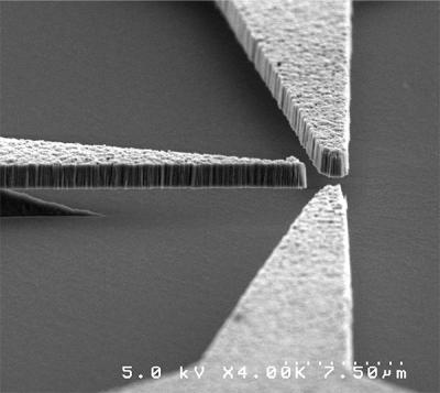
Scanning electron microscope image of a triode made from nanodiamond thin film that shows how the diamond components are cantilevered over a silicon dioxide substrate (credit: Davidson Laboratory, Vanderbilt University)
Electrical engineers at Vanderbilt University have developed all the basic components needed to create microelectronic devices out of thin films of nanodiamond, including diamond versions of transistors and, most recently, logical gates.
Diamond-based devices have the potential to operate at higher speeds and require less power than silicon-based devices, the engineers said. The nanodiamond circuits are a hybrid of old fashioned vacuum tubes and modern solid-state microelectronics, combining some of the best qualities of both technologies.
Potential applications include military electronics, circuitry that operates in space, ultra-high speed switches, ultra-low power applications, and sensors that operate in high radiation environments at extremely high temperatures (up to 900 degrees F) and extremely low temperatures (down to minus 300 degrees F).
The devices are so small that about one billion of them can be fabricated from one carat of diamond. The films are made from hydrogen and methane using a method called chemical vapor deposition that is widely used in the microelectronics industry for other purposes. This deposited form of diamond is less than one-thousandth the cost of “jewelry” diamond, which has made it inexpensive enough so that companies are putting diamond coatings on tools, cookware, and other industrial products. As a result, the cost of producing nanodiamond devices should be competitive with silicon, the researchers said.
Ref.: Nikkon Ghosh and Weng Poo Kang, Electronics Letters, Aug. 4 [link].