New 2D material could upstage graphene
March 25, 2016
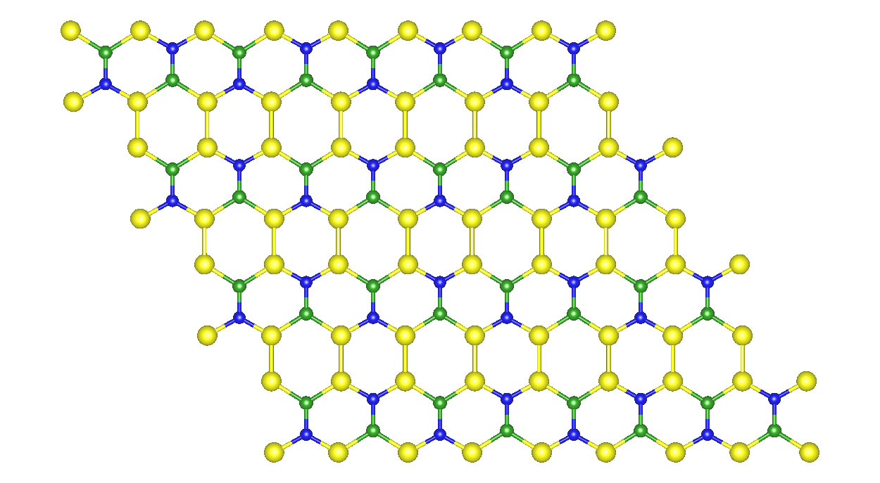
The atoms in the new structure are arranged in a hexagonal pattern as in graphene, but that is where the similarity ends. The three elements forming the new material all have different sizes; the bonds connecting the atoms are also different. As a result, the sides of the hexagons formed by these atoms are unequal, unlike in graphene. (credit: Madhu Menon)
A new one-atom-thick flat material made up of silicon, boron, and nitrogen can function as a conductor or semiconductor (unlike graphene) and could upstage graphene and advance digital technology, say scientists at the University of Kentucky, Daimler in Germany, and the Institute for Electronic Structure and Laser (IESL) in Greece.
Reported in Physical Review B, Rapid Communications, the new Si2BN material was discovered in theory (not yet made in the lab). It uses light, inexpensive earth-abundant elements and is extremely stable, a property many other graphene alternatives lack, says University of Kentucky Center for Computational Sciences physicist Madhu Menon, PhD.
Limitations of other 2D semiconducting materials
A search for new 2D semiconducting materials has led researchers to a new class of three-layer materials called transition-metal dichalcogenides (TMDCs). TMDCs are mostly semiconductors and can be made into digital processors with greater efficiency than anything possible with silicon. However, these are much bulkier than graphene and made of materials that are not necessarily earth-abundant and inexpensive.
Other graphene-like materials have been proposed but lack the strengths of the new material. Silicene, for example, does not have a flat surface and eventually forms a 3D surface. Other materials are highly unstable, some only for a few hours at most.
The new Si2BN material is metallic, but by attaching other elements on top of the silicon atoms, its band gap can be changed (from conductor to semiconductor, for example) — a key advantage over graphene for electronics applications and solar-energy conversion.
The presence of silicon also suggests possible seamless integration with current silicon-based technology, allowing the industry to slowly move away from silicon, rather than precipitously, notes Menon.
University of Kentucky | Dr. Madhu Menon Proposes New 2D Material
Abstract of Prediction of a new graphenelike Si2BN solid
While the possibility to create a single-atom-thick two-dimensional layer from any material remains, only a few such structures have been obtained other than graphene and a monolayer of boron nitride. Here, based upon ab initio theoretical simulations, we propose a new stable graphenelike single-atomic-layer Si2BN structure that has all of its atoms with sp2 bonding with no out-of-plane buckling. The structure is found to be metallic with a finite density of states at the Fermi level. This structure can be rolled into nanotubes in a manner similar to graphene. Combining first- and second-row elements in the Periodic Table to form a one-atom-thick material that is also flat opens up the possibility for studying new physics beyond graphene. The presence of Si will make the surface more reactive and therefore a promising candidate for hydrogen storage.