‘Pop-up’ fabrication technique trumps 3D printing
January 8, 2015

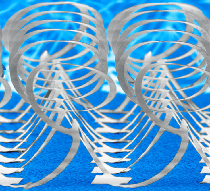
3D silicon microstructures formed using concepts similar to those in children’s “pop-up” books, shown here based on a colorized scanning electron micrograph (credit: University of Illinois College of Engineering)
Researchers at Northwestern University and the University of Illinois at Urbana-Champaign have developed a simple new fabrication technique to create beautiful, complex 3D micro- and nanostructures with advantages over 3D printing for a variety of uses.
The technique mimics the action of a children’s pop-up book — starting as a flat two-dimensional structure and popping up into a more complex 3D structure. Using a variety of advanced materials, including silicon, the researchers produced more than 40 different geometric designs, including shapes resembling a peacock, flower, starburst, table, basket, tent, and starfish.
“In just one shot you get your structure,” said Northwestern’s Yonggang Huang, one of three co-corresponding authors on the study. “We first fabricate a two-dimensional structure on a stretched elastic material. Then we release the tension, and up pops a 3-D structure. The 2-D structure must have some place to go, so it pops up.”

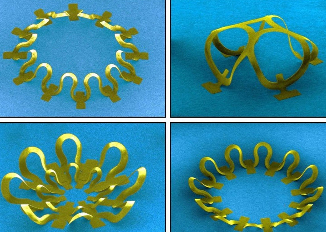
Experimental images of flower-like structures formed from a two-dimensional structure transferred onto a stretched elastic material. When the tension is released, the desired 3-D structure forms by popping up. (Credit: University of Illinois)
The pop-up assembly technique is expected to be useful in building biomedical devices, sensors and electronics. It is the current cover story in the Jan. 9 issue of the journal Science.
Determining which designs are needed for specific applications will come in future research.
Huang, who led the portion of the research focused on theory, design and modeling, is the Joseph Cummings Professor of Civil and Environmental Engineering and a professor of mechanical engineering at Northwestern’s McCormick School of Engineering and Applied Science.
The new pop-up method, which is based on compression buckling, is fast and inexpensive, and can be used to build many different structures at one time. It uses many different materials, including silicon, incorporating different materials into one hybrid structure. It can be used to build structures on both micro- and nano-levels (down to a thickness of 100 nanometers), and can produce a wide range of different geometries.
With 3-D printing, on the other hand, it is difficult to integrate more than one material in a structure; it is almost impossible to print semiconductors or single crystalline metals; and speed is slow.
“We know how to design a 2D structure so that it pops up into the 3D structure we desire,” said Yihui Zhang, a co-corresponding author of the study. Zhang, who is a research assistant professor of civil and environmental engineering at Northwestern, came up with the initial idea.
Zhang worked together with the research group of John A. Rogers, the paper’s third co-corresponding author and a Swanlund Chair and professor of materials science and engineering at the University of Illinois, in developing the structural designs of 2-D structures to form various classes of 3-D configurations.

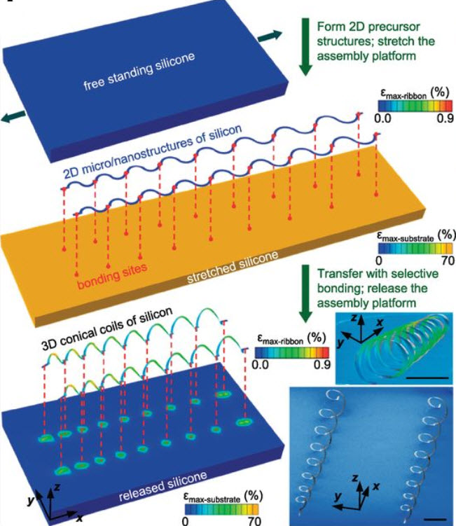
Process for deterministic assembly of 3D mesostructures of monocrystalline silicon from 2D precursors. The technique combines strong points of adhesion and weak points of adhesion between the 2D structure and the elastomer it is placed on. When the stretch is released, compression buckling takes place. The strong adhesion points stay in the plane of the elastomer, while the weak points break away. The intended structure pops up into three dimensions. Zhang used a mechanics model to predict how strong the adhesion points needed to be for a given design. (Credit: Sheng Xu et al./Science)
“A key, unique feature of these approaches to 3-D microarchitectures is that they work equally well with a very wide variety of materials, including the highest performance semiconductors, such as device-grade silicon, and fully formed, state-of-the-art planar devices and systems,” said Rogers. “We believe, as a result, that these ideas have relevance to nearly every class of microsystem technology — from electronics to photonics, optoelectronics, microelectromechanical structures and others.”
Rogers, who also is director of the Seitz Materials Research Laboratory, led the group that worked on the experimental and fabrication work of the different structures, as well as the device demonstration. Rogers, Huang and Zhang, together with postdoctoral fellows, led the development of the concepts in the 3-D fabrication approach.
Scientists at Zhejiang University, Hangzhou, China; Hanyang University, Seoul, Korea; and East China University of Science and Technology, Shanghai were also involved in the study. The U.S. Department of Energy supported the research.
Abstract for Assembly of micro/nanomaterials into complex, three-dimensional architectures by compressive buckling
Complex three-dimensional (3D) structures in biology (e.g., cytoskeletal webs, neural circuits, and vasculature networks) form naturally to provide essential functions in even the most basic forms of life. Compelling opportunities exist for analogous 3D architectures in human-made devices, but design options are constrained by existing capabilities in materials growth and assembly. We report routes to previously inaccessible classes of 3D constructs in advanced materials, including device-grade silicon. The schemes involve geometric transformation of 2D micro/nanostructures into extended 3D layouts by compressive buckling. Demonstrations include experimental and theoretical studies of more than 40 representative geometries, from single and multiple helices, toroids, and conical spirals to structures that resemble spherical baskets, cuboid cages, starbursts, flowers, scaffolds, fences, and frameworks, each with single- and/or multiple-level configurations.