Quantum dot solids: a new era in electronics?
February 26, 2016

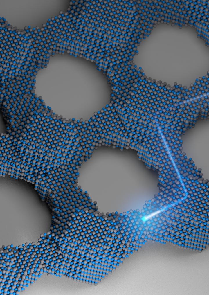
Connecting the dots: Playing ‘LEGO’ at the atomic scale to build atomically coherent quantum dot solids (credit: Kevin Whitham, Cornell University)
Just as the single-crystal silicon wafer forever changed the nature of communication 60 years ago, Cornell researchers hope their work with quantum dot solids — crystals made out of crystals — can help usher in a new era in electronics.
The team has fashioned two-dimensional superstructures out of single-crystal building blocks. Using a pair of chemical processes, the lead-selenium nanocrystals are synthesized into larger crystals, then fused together to form atomically coherent square superlattices.
Cornell University | Quantum dot solids
The difference between these and previous crystalline structures is the atomic coherence of each 5-nanometer crystal (a nanometer is one-billionth of a meter). They’re not connected by a substance between each crystal — they’re connected to each other directly. The electrical properties of these superstructures are potentially superior to existing semiconductor nanocrystals, with anticipated applications in energy absorption and light emission.
“As far as level of perfection, in terms of making the building blocks and connecting them into these superstructures, that is probably as far as you can push it,” said Tobias Hanrath, associate professor in the Robert Frederick Smith School of Chemical and Biomolecular Engineering, referring to the atomic-scale precision of the process.
The Hanrath group’s paper, “Charge transport and localization in atomically coherent quantum dot solids,” is published in this month’s issue of Nature Materials.
The strong coupling of the nanocrystals leads to formation of energy bands that can be manipulated based on the crystals’ makeup, and could be the first step toward discovering and developing other artificial materials with controllable electronic structure.
The structure of the Hanrath group’s superlattice, while superior to ligand-connected nanocrystal solids, still has multiple sources of disorder due to the fact that all nanocrystals are not identical. This creates defects, which limit electron wave function.
This work made use of the Cornell Center for Materials Research, which is supported by the National Science Foundation through its Materials Research Science and Engineering Center program. X-ray scattering was conducted at the Cornell High Energy Synchrotron Source, which is supported by the NSF and the National Institutes of Health.
Abstract of Charge transport and localization in atomically coherent quantum dot solids
Epitaxial attachment of quantum dots into ordered superlattices enables the synthesis of quasi-two-dimensional materials that theoretically exhibit features such as Dirac cones and topological states, and have major potential for unprecedented optoelectronic devices. Initial studies found that disorder in these structures causes localization of electrons within a few lattice constants, and highlight the critical need for precise structural characterization and systematic assessment of the effects of disorder on transport. Here we fabricated superlattices with the quantum dots registered to within a single atomic bond length (limited by the polydispersity of the quantum dot building blocks), but missing a fraction (20%) of the epitaxial connections. Calculations of the electronic structure including the measured disorder account for the electron localization inferred from transport measurements. The calculations also show that improvement of the epitaxial connections will lead to completely delocalized electrons and may enable the observation of the remarkable properties predicted for these materials.