Researchers unravel the secret to making cheap, high-density data storage
October 11, 2012

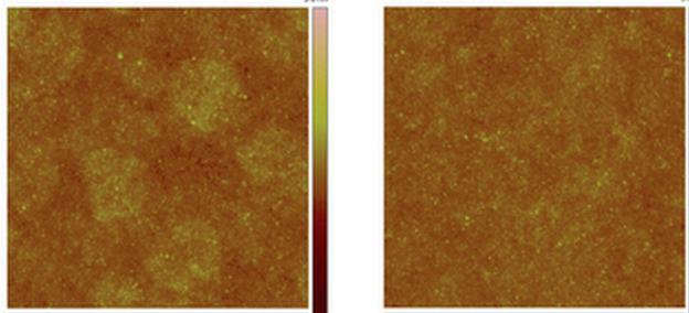
Magnetic media with (right) and without (left) a smoothing layer (credit: Shreya Kundu, et al./Scientific Reports)
Researchers from A*STAR’s Institute of Materials Research and Engineering (IMRE) and the National University of Singapore (NUS) have discovered that an ultra-smooth surface is the key factor for “self-assembly” — a cheap, high-volume, high-density patterning technique for data storage.
This technique allows manufacturers to use the method for data storage on a variety of different surfaces. This discovery paves the way for the development of next-generation data storage devices, with capacities of up to 10 Terabits per square inch, which could lead to significantly greater storage on much smaller data devices.
The “self-assembly” technique is one of the simplest and cheapest high-volume methods for creating uniform, densely-packed nanostructures that could potentially help store data.
Self-assembly is one of the leading candidates for large scale nanofabrication at very high pattern densities. One of its most obvious applications will be in the field of bit-patterned media for the hard disk industry.
It is widely used in research and is gaining acceptance in industry as a practical lithographic tool for sub-100 nm, low-cost, large area patterning. However, attempts to employ self-assembly on different surface types, such as magnetic media used for data storage, have shown varying and erratic results to date. This phenomenon has continued to puzzle industry researchers and scientists globally.
Researchers from A*STAR’s IMRE and NUS have now solved this mystery and identified that the smoother the surface, the more efficient the self-assembly of nanostructures will be. This breakthrough allows the method to be used on more surfaces and reduce the number of defects in an industrial setting. The more densely packed the structures are in a given area, the higher the amount of data that can be stored.
The team discovered that a height of 5 angstroms (the width of about 5 atoms) RMS (root mean square) roughness was the maximum surface roughness allowed for successful self-assembly of dots, which could eventually be used in making high-density data storage.
“If we want large scale, large area nanopatterning using very affordable self-assembly, the surface needs to be extremely smooth so that we can achieve efficient, successful self-assembly with lower incidences of defects.”
The discovery was recently published in Scientific Reports, an open access journal from Nature.
This research is supported by the National Research Foundation Singapore under its “Frontier in magnetic recording research: Vision for 10 terabits per square inch” programme (NRF-CRP 002-097 NRF-08) and administered by A*STAR’s IMRE.