Computer memory that can store about one terabyte of data on a device the size of a postage stamp
July 14, 2014

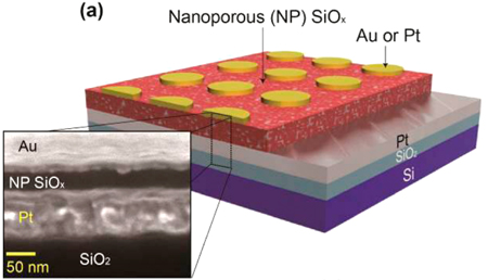
This scanning electron microscope image and schematic show the design and composition of new RRAM memory devices based on porous silicon oxide that were created at Rice University (credit: Tour Group/Rice University)
High-density, next-generation computer memory that can store about one terabyte of data on a device the size of a postage stamp — more than 50 times the data density of current flash memory technology — is now a step closer to mass production.
That’s because Rice University’s breakthrough silicon oxide technology will allow manufacturers to fabricate “resistive random-access memory” (RRAM) devices at room temperature with conventional production methods, the researchers say.
In a new paper in Nano Letters, a Rice team led by chemist James Tour compared its RRAM technology to more than a dozen competing versions.
“This memory is superior to all other two-terminal unipolar resistive memories by almost every metric,” Tour said. “And because our devices use silicon oxide — the most studied material on Earth — the underlying physics are both well-understood and easy to implement in existing fabrication facilities.” Tour is Rice’s T.T. and W.F. Chao Chair in Chemistry and professor of mechanical engineering and nanoengineering and of computer science.
How resistive memory works
The basic concept behind resistive memory devices is the insertion of a dielectric material — one that won’t normally conduct electricity — between two wires. When a sufficiently high voltage is applied across the wires, a narrow conduction path can be formed through the dielectric material.

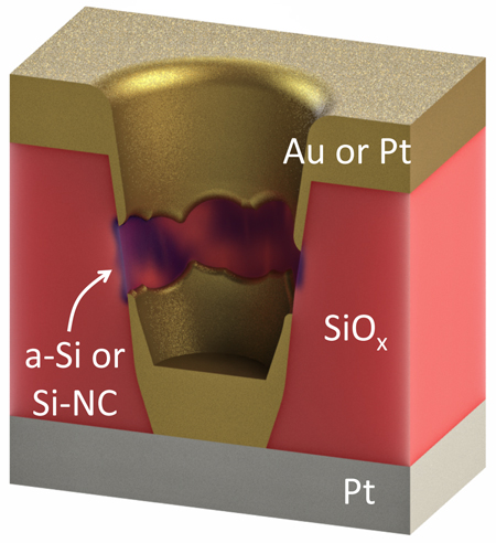
This illustration depicts the rewriteable crystalline filament pathway in Rice University’s porous silicon oxide RRAM memory devices (credit: Tour Group/Rice University)
The presence or absence of these conduction pathways can be used to represent the binary 1s and 0s of digital data.
Research with a number of dielectric materials over the past decade has shown that such conduction pathways can be formed, broken and reformed thousands of times, which means RRAM can be used as the basis of rewritable random-access memory.
RRAM is under development worldwide and expected to supplant flash memory technology in the marketplace within a few years because it is faster than flash and can pack far more information into less space.
Improving RRAM
Tour and colleagues began work on their breakthrough RRAM technology more than five years ago. The key ingredient of Rice’s RRAM is its dielectric component, silicon oxide. Silicon is the most abundant element on Earth and the basic ingredient in conventional microchips.
Microelectronics fabrication technologies based on silicon are widespread and easily understood, but until the 2010 discovery of conductive filament pathways in silicon oxide in Tour’s lab, the material wasn’t considered an option for RRAM.
Since then, Tour’s team has raced to further develop its RRAM and even used it for exotic new devices like transparent flexible memory chips.

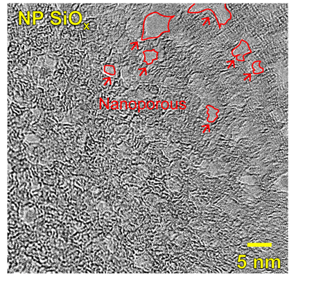
This electron microscope image shows the surface of the nanoporous silicon-oxide material used in Rice University’s new RRAM memory devices. The red areas highlight gaps, or voids, in the material’s amorphous silicon-oxide coating. (Credit: Tour Group/Rice University)
“Our technology is the only one that satisfies every market requirement, both from a production and a performance standpoint, for nonvolatile memory,” Tour said.
“It can be manufactured at room temperature, has an extremely low forming voltage, high on-off ratio, low power consumption, nine-bit capacity per cell, exceptional switching speeds and excellent cycling endurance.”
In the latest study, a team headed by lead author and Rice postdoctoral researcher Gunuk Wang showed that using a porous version of silicon oxide could dramatically improve Rice’s RRAM in several ways.
First, the porous material reduced the forming voltage — the power needed to form conduction pathways — to less than two volts, a 13-fold improvement over the team’s previous best and a number that stacks up against competing RRAM technologies. In addition, the porous silicon oxide also allowed Tour’s team to eliminate the need for a “device edge structure.”
“That means we can take a sheet of porous silicon oxide and just drop down electrodes without having to fabricate edges,” Tour said. “When we made our initial announcement about silicon oxide in 2010, one of the first questions I got from industry was whether we could do this without fabricating edges. At the time we could not, but the change to porous silicon oxide finally allows us to do that.
“We also demonstrated that the porous silicon oxide material increased the endurance cycles more than 100 times as compared with previous nonporous silicon oxide memories. Finally, the porous silicon oxide material has a capacity of up to nine bits per cell that is highest number among oxide-based memories, and the multiple capacity is unaffected by high temperatures.”
Tour said the latest developments with porous silicon oxide — reduced forming voltage, elimination of need for edge fabrication, excellent endurance cycling and multi-bit capacity — are extremely appealing to memory companies.
“This is a major accomplishment, and we’ve already been approached by companies interested in licensing this new technology,” he said.
Abstract of Nano Letters paper
Oxide-based two-terminal resistive random access memory (RRAM) is considered one of the most promising candidates for next-generation nonvolatile memory. We introduce here a new RRAM memory structure employing a nanoporous (NP) silicon oxide (SiOx) material which enables unipolar switching through its internal vertical nanogap. Through the control of the stochastic filament formation at low voltage, the NP SiOx memory exhibited an extremely low electroforming voltage ( 1.6 V) and outstanding performance metrics. These include multibit storage ability (up to 9-bits), a high ON–OFF ratio (up to 107 A), a long high-temperature lifetime (≥104 s at 100 °C), excellent cycling endurance (≥105), sub-50 ns switching speeds, and low power consumption (
 6 × 10⁻⁵ W/bit). Also provided is the room temperature processability for versatile fabrication without any compliance current being needed during electroforming or switching operations. Taken together, these metrics in NP SiOx RRAM provide a route toward easily accessed nonvolatile memory applications.