Nanowire-bridging transistors open way to next-generation electronics
May 19, 2014

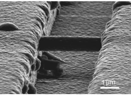
EM image of a nanobridge channel (credit: UC Davis)
Taking the next step beyond silicon integrated circuits, engineers at the University of California, Davis have developed a new approach that allows nonsilicon nanowires and other nanostructures to be combined with silicon surfaces.
It shows promise for a new generation of fast, robust electronic and photonic devices.
Bypassing silicon’s limits
Circuits built on conventionally etched silicon have reached their lower size limit, which restricts operation speed and integration density. And conventional silicon circuits cannot function at temperatures above 250 degrees Celsius (about 480 degrees Fahrenheit), or handle high power or voltages, or optical applications.
The new technology could be used, for example, to build sensors and control systems that can operate under high temperatures, such as in motor vehicles, boats, airplanes, terrestrial oil and ore extraction, rockets, spacecraft, and bodily implants,” said Saif Islam, professor of electrical and computer engineering at UC Davis.

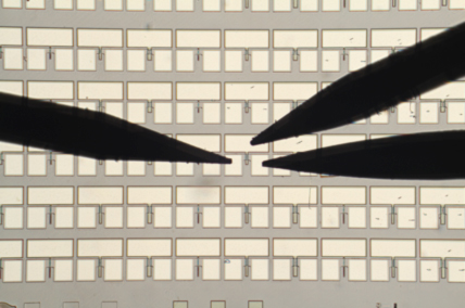
Nanobridge device array (credit: UC Davis)
How to grow nonsilicon materials
Conventional microcircuits are formed from etched layers of silicon and insulators, but it’s difficult to grow nonsilicon materials as layers over silicon because of incompatibilities in crystal structure (“lattice mismatch”) and differences in thermal properties.
Instead, Islam’s laboratory at UC Davis has created silicon wafers with “nanopillars” of materials such as gallium arsenide, gallium nitride or indium phosphide on them, and grown tiny nanowire “bridges” between nanopillars.
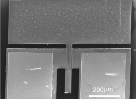
The researchers have been able to make these nanowires operate as transistors, and combine them into more complex circuits as well as devices that are responsive to light. They have developed techniques to control the number of nanowires, their physical characteristics, and consistency.
Islam said the suspended structures have other advantages: they are easier to cool and handle thermal expansion better than planar structures — a relevant issue when mismatched materials are combined in a transistor.

EM image of a nanobridge transistor (credit: UC Davis)
The technology also leverages the well-established technology for manufacturing silicon integrated circuits, instead of having to create an entirely new route for manufacturing and distribution, Islam said.
The work is described in a series of recent papers in the journals Advanced Materials, Applied Physics Letters and IEEE Transactions on Nanotechnology.
Co-authors include engineers at the University of Incheon, South Korea, and Kwangwoon University, South Korea. Funding was provided by the U.S. National Science Foundation and the government of South Korea.
UC Davis engineers are building new circuits with transistors made of semiconductor nanowires grown on silicon. These circuits have new capabilities, such as handling light or heat resistance, while retaining the manufacturing advantages of silicon.
Abstract of Advanced Materials paper
Integrated surround-gate field-effect-transistors enabled by bottom-up synthesis of nano-bridges are demonstrated. Horizontally oriented silicon nano-bridge devices are fabricated avoiding the rigorous processes for aligning and contacting nanowires grown via a bottom-up technique. Evaluation of electrical properties and a memory device application of the transistors are presented.
Abstract of Applied Physics Letters paper
We fabricated photosensitive silicon-nanobridge 3-D field-effect-transistors and demonstrated their analog and digital applications. The channels of the transistors were implemented by nanowires, grown and bridged between pairs of silicon electrodes using the vapor-liquid-solid technique. Whilst characteristics of the nanowire transistor such as the inverse sub-threshold slopes, the on-current, and the threshold voltage remained nearly unaffected by illumination, magnitude of the off-current was significantly increased by up to three orders of magnitude with increasing intensity. Such off-current modulation enabled by illumination offers opportunities for applications such as electro-optical OR gate circuit elements and frequency doublers.
Abstract of IEEE Transactions on Nanotechnology paper
Nanowire bridges are attractive structures for characterizing nanowires without impairment during the postprocessing steps and fabricating high-performance sensors. In this study, arrays of silicon nanowire bridges were reproducibly fabricated using chemical vapor deposition in the confined regions of patterned silicon electrodes. While depositing gold colloids without additives resulted in a negligible number of nanowire bridges, treating the colloids with HF acid or functionalizing the silicon electrode surfaces with poly-L-lysine increased the yields to nearly 97%. This dramatic improvement in yield was a result of increased adsorption of Au nanoparticles to the electrode surface. We show that diluted colloids along with the electrode surface treatment increase the possibility of occurrence of bridges with fewer nanowires. Micrographs and current-voltage measurements showed robust electrical, mechanical and metallurgical connections of nanowire bridges to the electrodes during the growth process.